George Lisensky (Beloit College) and Christopher Bailey (Wells College)
This workshop was offered July 26-31, 2015 by George Lisensky and Christopher Bailey at Beloit College.
It was previously offered in 2013 by George Lisensky and Christopher Bailey,
in 2011 by David Brown at Southwestern College, and in 2004, 2005, 2007, and 2009 by George Lisensky and Karen Nordell.
In 1960, Richard Feynman asked the question, “What would happen if we could arrange atoms one by one the way we want them?” Today, the emerging fields of nanoscience and nanotechnology are enabling control of the material world at the scale of atoms and molecules.
Nanotechnology is inherently interdisciplinary and requires new approaches to undergraduate education through interdisciplinary connections between chemistry, physics, biology and materials science. Chemists can play an important part in this collaboration if the barrier of unfamiliar vocabulary is removed.
Silicon chips, gigabyte disk drives, and light emitting diodes - devices that are based on atomically engineered materials - are all around us. These everyday wonders that we depend on would not be possible without the ability to "see" and manipulate materials at the most basic level, the individual atom.
This workshop will focus on a chemical view of materials science and the nanoworld and how to incorporate these topics into the core curriculum. It will include a large number of hands-on activities, connections to commercial high technology materials, and laboratory experiments that do not require specialized equipment. Participants will receive a book, lab directions, and resources for class use.
Day 1: What’s different about the nanoscale?
Topics: Introduction to Nanoscale Materials; Nanoapplications; Superhydrophobicity; Electrons in
Solids (Magnetism, Giant Magnetoresistance, Data Storage); Metal Nanoparticles
Laboratory Activities: Property changes from a monolayer; Electrochromic Prussian Blue; Synthesis of ferrofluid nanoparticles; Synthesis of gold
and silver nanoparticles
Day 2: Materials chemistry
Topics: Solid state stoichiometry; Unit cells; Carbon; Metals, bands and semiconductors; Quantum Dots
Laboratory Activities: Structure and properties model building; Thermal conductivity;
Preparation of ZnO nanorods; Titanium dioxide dye solar cell
Day 3: How can we use the periodic table to tune properties?
Topics: Periodic properties and solid solutions; Light Emitting Diodes and applications; p-n junctions; Solar cells; Thermoelectrics
Laboratory Activities: LEDs and periodic properties; Liquid crystal thermometer; Preparation of OLEDs; Synthesis of CdSe quantum
dots
Day 4: How do we know about structure?
Topics: Diffraction; DNA
diffraction; Scanning Probe Microscopy; Piezoelectricity
Laboratory Activities: Optical Transforms; CH3NH3PbX3 perovskite solid solutions; Properties of ZnO nanorods
Day 5: Defects and Society
Topics and activities: Dislocations; Bubble raft; Amorphous
metal; Societal implications; Conclusion
Dates
The workshop schedule runs from dinner at 6:00 pm on Sunday, July 26, through lunch on Friday, July 31, 2015.
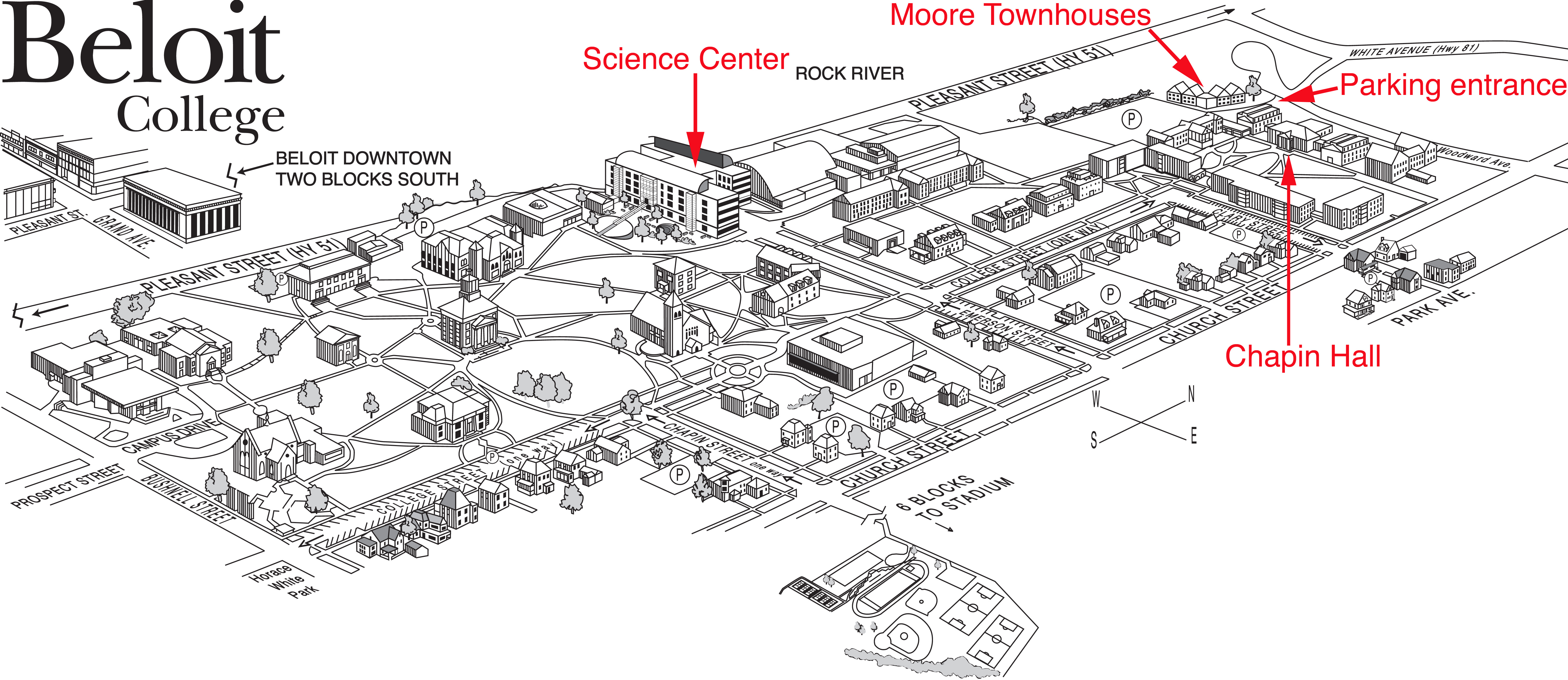
Travel by air
The Chicago O'Hare airport (ORD) is 85 miles from Beloit. There is almost hourly airport bus service available for $28 each way. See https://www.govangalder.com/assets/June_2017_schedule.pdf for a schedule. If you give us your travel plans we will meet the Van Galder bus in South Beloit, Illinois and take you to campus. Milwaukee (70 miles) and Madison (50 miles) airports are also nearby but no public transportation is available from those locations.
Travel by car
Beloit is located at the border between Wisconsin and Illinois at
the intersection of Interstate 90 and Interstate 43. There is no charge for parking on campus during the workshop.
Driving Directions